Skip to content
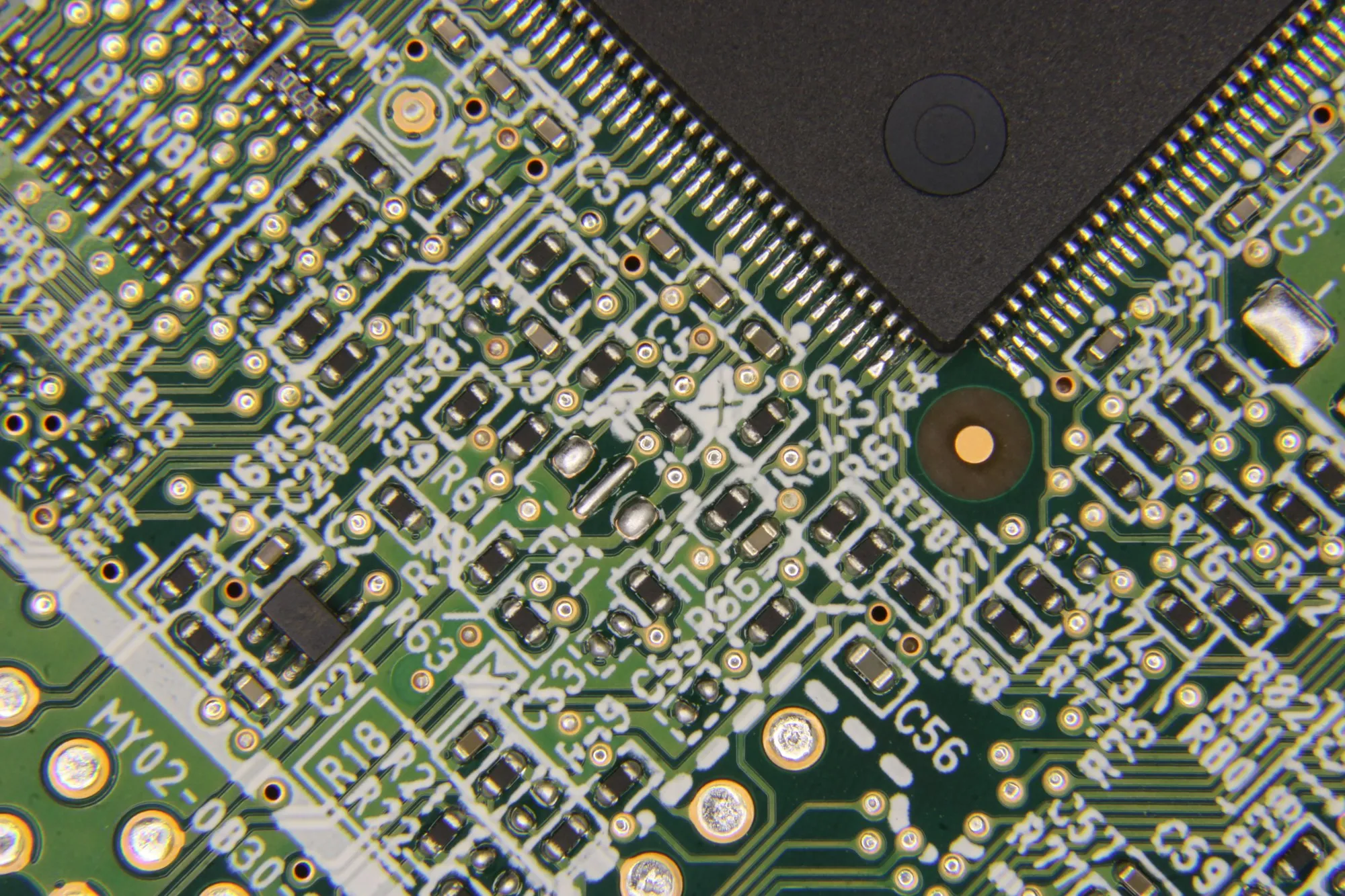
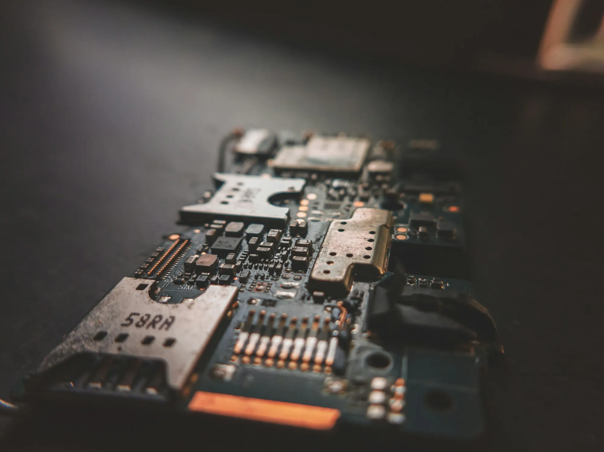
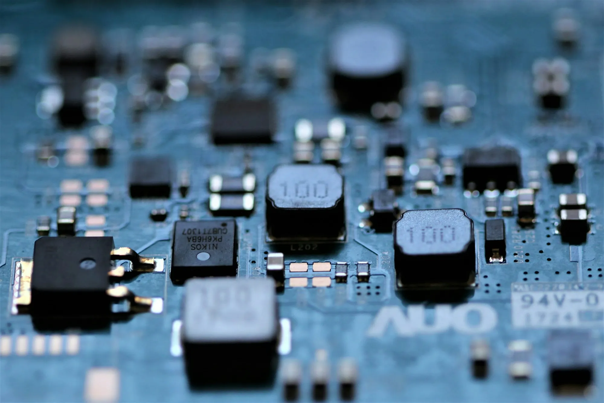
Hardware detail of a black and grey control mainboard

FPGA / MCU control architecture

FPGA for the real-time display path, MCU for device control

FPGA and MCU are not interchangeable marketing words but engineering tools at different levels. The registers, command packets, boot sequence, status readback and factory commands between them are defined together.

FPGA
Timing / mapping / interface
MCU
Command / status / test
Engineering goal
Debuggable, traceable, manufacturable

THE SPLIT

How FPGA and MCU divide the work

FPGA and MCU are not interchangeable marketing words. They are engineering tools at different levels. The FPGA suits real-time, high-speed, parallel and timing-sensitive work: display data organisation, pixel mapping, interface bridging, row/column timing, receiving-side output and test-pattern generation.

The MCU suits state management, peripheral control, communication protocol, parameter storage, fault records, programming and production test. In a real project the two usually work together: the FPGA owns the real-time display path, the MCU owns configuration, monitoring and maintenance.

The judgement that matters is whether a project needs an FPGA at all, whether an MCU alone is enough, whether an existing main controller plus an interface board would do, or whether a full sending/receiving chain is required. Small cost-sensitive products should not be over-designed; high-resolution or multi-module projects should not be forced through a low-cost control path.

FPGA

Real-time display path

  • Display data organisation and pixel mapping
  • Row/column timing and output refresh
  • Interface bridging and receiving-side output
  • Test-pattern generation and debug registers

MCU

Device control and maintenance

  • Command-packet transport and parameter storage
  • Status readback, temperature and voltage monitoring
  • Fault codes, watchdog and abnormal recovery
  • Programming, version readout and factory-test commands

BUILD ORDER

Four key faces

Four key faces of the integrated control architecture

Compile efficiency, packet format, handshake and test protocol are what real projects run into, and where a pilot build succeeds or stalls.

FPGA compile efficiency and iteration control
01

FPGA compile efficiency and iteration control

A practical FPGA workflow separates display timing, pixel mapping, interface bridges and debug registers so changes can be compiled, tested and tracked without destabilizing the whole design.

  • Module-level constraints and reusable timing blocks
  • Test-pattern logic for board bring-up
  • Versioned bitstreams and board validation notes
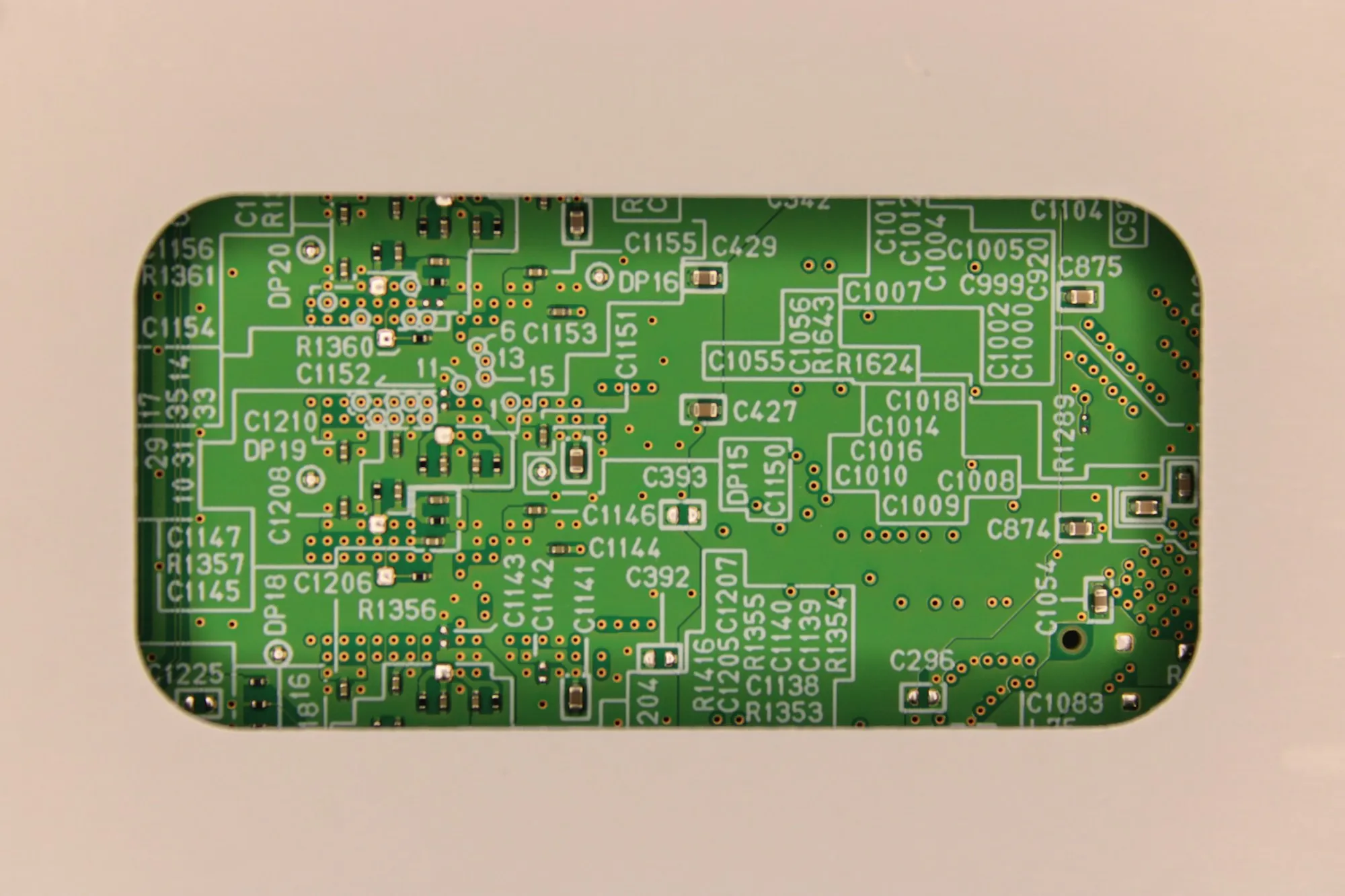
MCU packet format and command transport
02

MCU packet format and command transport

MCU protocols should define frame header, command ID, payload length, version, checksum, ACK/NACK, timeout and retry rules for factory test and field diagnostics.

  • UART/SPI/I2C/Ethernet command framing
  • Register read/write and status packets
  • Error code, version and production-test commands
FPGA and MCU handshake
03

FPGA and MCU handshake

The FPGA handles real-time display paths while the MCU configures modes, reads status, manages startup and exposes service commands.

  • Register map between MCU and FPGA
  • Mode switch, reset and boot sequencing
  • Temperature, voltage and link-state readback
Production-test protocol
04

Production-test protocol

A manufacturable control board needs commands for programming, version readout, test images, interface checks, fault capture and result logging.

  • Factory programming and serial-number binding
  • Display output and interface self-test
  • Failure classification for pilot production

TECHNICAL TOPICS

Judgement along the chain

Input, timing, mapping and diagnostics

Each topic states what has to be confirmed, what engineering judgement is applied and how it is verified on the prototype.

01

Signal input and interface adaptation

Confirm the content source, interface type, colour format and host environment first, then match the input interface to the display chain behind it.

Engineering checks

  • Player board, industrial PC, media box or custom controller output timing
  • Interface stability, cable distance and connector direction
  • Start-up order and recovery after an unexpected disconnect
02

Clock, sync and display timing

Stability depends on clock, reset, sync and output timing. Where a project needs multi-panel sync or low latency, the test conditions are defined during architecture and verified on the prototype.

Engineering checks

  • Clock path and reset behaviour
  • Frame boundary and output refresh
  • Recovery from abnormal states
03

Pixel mapping and receiving-side allocation

Advertising and LED projects involve module layout, cabinet zoning and receiving-side load. Physical layout is translated into a control chain that can be diagnosed and tested.

Engineering checks

  • Which area each receiving side drives, and how it is connected
  • How a fault is located when one region misbehaves
  • How production test covers every output channel
04

Status monitoring and fault diagnosis

Where the project needs it, temperature, voltage, communication status, version readout, fault codes and a debug interface are reserved during design so problems can be located in production and in the field.

Engineering checks

  • Temperature, voltage and link-state readback
  • Firmware/logic version reporting
  • Fault codes and a reachable debug interface

PACKET FORMAT

MCU command transport

Packet structure decides whether the line and the field can locate a fault

No customer protocol is published here. The fields below show the kind of structure and exception handling considered when command transport is designed.

  1. 00 header
  2. 01 version
  3. 02 command ID
  4. 03 length
  5. 04 payload
  6. 05 checksum
  7. 06 ACK / NACK
  8. 07 error code
  9. 08 timeout
  10. 09 retry

Illustrative fields only, not any customer protocol. Real fields, widths, timeout strategy and exception handling are defined per project and verified on the prototype.

IN THE CHAIN

System view

Where FPGA and MCU sit in the chain

The FPGA is not isolated and the MCU is not a helper chip; both are defined together with input, sending, receiving, modules and production test.

  1. 01 Signal Input
  2. 02 FPGA / MCU Control
  3. 03 Sending / Output Unit
  4. 04 Transmission Link
  5. 05 Receiving / Module Control
  6. 06 Display Output
  7. 07 Production Test
HQControl works across the whole chain rather than a single board. The interface, timing and test boundary of each stage is defined during architecture.

FPGA WORKFLOW

Compile efficiency comes from module boundaries and validation strategy

A display FPGA project should avoid tightly coupled logic. Input interfaces, pixel mapping, timing output, test patterns, debug registers and board interfaces are kept separate so a local change does not destabilise the whole design.

Each bitstream is tied to a board version, constraint files, test notes and an issue list — so what is visible is iteration speed, debugability, version tracking and prototype validation rather than the phrase “high-speed FPGA”.

Project inquiry

Turn display requirements into validated, manufacturable control hardware

Share display type, target specifications, interface requirements and project stage. We review the control hardware approach and ODM cooperation model; pricing and lead time follow project review.

Helpful to include

  • Screen size, pixel pitch, module layout and target resolution
  • Input source, control distance, sending/receiving count and cabling
  • Enclosure space, connector direction, power, temperature rise and service access
  • Test patterns, long-run checks, restart recovery and the factory-test standard
  • Existing boards, BOM, schematics or fault samples, if any
  • Estimated volume, project stage and target schedule