Skip to content
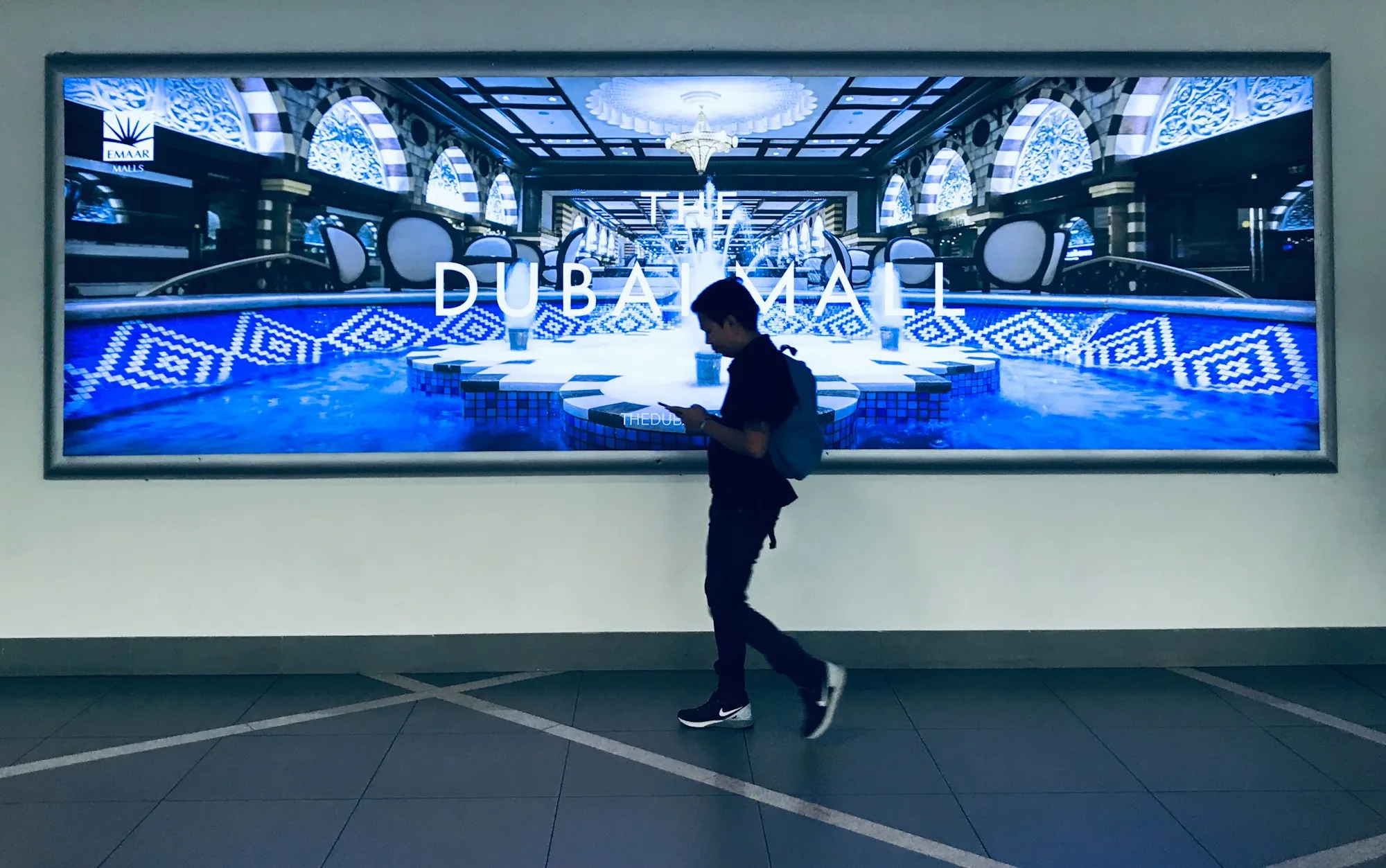
Large-format digital displays in a technical exhibition environment, used as context for display and imaging-interface engineering.

Engineering

Display control, imaging interfaces and hardware validation

FPGA and MCU control architecture, interface and firmware adaptation, and the validation work that decides whether a board is ready for a customer product.

Why a display device needs dedicated control hardware capability

Advertising screens, commercial displays, small display products and large LED display systems all look like “a screen”. What actually decides whether the product runs stably is the control hardware behind it.

The customer sees brightness, picture, response, stability, interfaces and appearance. The engineering team faces the signal chain, timing, bandwidth, power, thermal behaviour, structure, firmware, test and supply chain.

Control hardware does not need to be as complex or as high-spec as possible — it needs to suit the product target. A retail signage project may weight cost, stability and peripheral control; an outdoor LED project may weight the receiving side, reliability, batch consistency and service access.

FPGA & MCU Control

FPGA & MCU control

FPGA handles high-speed display paths, timing and interface conversion; MCU handles device state, peripherals, communication and production-test entry.

High-Speed FPGA Display Control Architecture

FPGA-centred handling of high-speed display links, timing control, pixel channels, interface conversion and complex display structures.

  • Define the FPGA control core, input/output links and board interfaces around the display product target.
  • Build hardware logic for high-speed data, pixel channels, timing control and interface conversion.
  • Suitable for sending-side control, receiving-side links, display-module control and custom display structures.
  • Confirm display output, link stability and manufacturability through prototype bring-up and validation.
MCU Device Control and Interface Management

MCU-based device-state control, peripheral coordination, communication interfaces, user operation and complete-device logic.

  • Covers keys, sensing, communication, power state, peripheral control and device-level coordination.
  • Combines with FPGA display links, sending cards, receiving cards and interface boards into a complete control unit.
  • Supports prototype debugging, firmware-level fault location, production-test entry and status feedback logic.
  • Suits advertising screens, commercial displays, small display products and custom devices.

Sending Card and Receiving Card Signal-Chain Capability

Organise sending cards, receiving cards and display control modules around input, processing, distribution, transmission and display-side control.

  • Sending cards, receiving cards and display control modules are defined inside the complete signal chain.
  • The requirement is broken down by input, processing, output, transmission, receiving and display side.
  • Control hardware can be defined around advertising screens, commercial displays, LED modules and custom devices.
  • Specification, loading, interface, refresh and sync figures are published only after project verification.

Display control chain

HQControl works across the whole chain — input, control core, sending/output, transmission, receiving/module control, display output and production test.

  1. 01 Signal Input
  2. 02 FPGA / MCU Control
  3. 03 Sending / Output Unit
  4. 04 Transmission Link
  5. 05 Receiving / Module Control
  6. 06 Display Output
  7. 07 Production Test
HQControl works across the whole chain rather than a single board. The interface, timing and test boundary of each stage is defined during architecture.
  • Signal input and interface adaptation

    Confirm the content source, interface type, colour format and host environment first, then match the input interface to the display chain behind it.

  • Clock, sync and display timing

    Stability depends on clock, reset, sync and output timing. Where a project needs multi-panel sync or low latency, the test conditions are defined during architecture and verified on the prototype.

  • Pixel mapping and receiving-side allocation

    Advertising and LED projects involve module layout, cabinet zoning and receiving-side load. Physical layout is translated into a control chain that can be diagnosed and tested.

  • Display output, greyscale and colour verification

    Display quality is broken into verifiable items rather than headline figures: test patterns, greyscale transition, low-brightness behaviour, colour consistency and stable refresh.

  • Status monitoring and fault diagnosis

    Where the project needs it, temperature, voltage, communication status, version readout, fault codes and a debug interface are reserved during design so problems can be located in production and in the field.

  • BOM and component sourcing

    A control-hardware BOM is judged on supply lead time, alternatives, electrical margin, package, temperature range, assembly process and batch stability — not on function alone.

  • Production test and version traceability

    Production test enters the design early: test points and programming headers at PCB stage, test commands and version readout at firmware stage, pass/fail criteria and records at production stage.

  • Documentation and project handover

    An ODM project does not end at a prototype. Requirement confirmation, architecture notes, schematic/PCB/BOM, interface definition, firmware version, test records and revision history are what let a customer keep maintaining and iterating the product.

High-Speed Imaging & FAT Experience

High-Speed Imaging and FAT Hardware Engineering

Sensor interfaces, FPGA data paths, trigger synchronization and complete-device hardware integration for high-speed cameras, automatic timing and custom imaging equipment.

HQControl's chief engineer previously led the hardware design of complete FAT (Fully Automatic Timing) systems. This capability is presented as the chief engineer's prior system-level experience, not as an HQControl-owned FAT product or customer case.

  • High-speed camera and image-sensor interfaces
  • Chinese sensor and imaging-chip adaptation
  • FPGA image acquisition and processing data paths
  • MIPI CSI-2 and HDMI interface development
  • Multi-camera switching, binning and picture-in-picture
  • Triggering, timing and hardware synchronization
  • Complete-device hardware integration

Customer types

  • High-speed camera developers
  • Automatic timing and sensing-system companies
  • Custom-imaging OEMs

Publication boundaries

Specific frame rate, resolution, interface and system performance figures are confirmed per publishable project material or new-project validation results — not published as generic specifications.

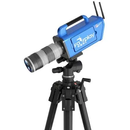
A complete FAT finish-line camera system representative of hardware previously led by HQControl’s chief engineer; it is not presented as an HQControl-owned product.

Interface & Firmware Adaptation

Interface & Firmware Adaptation

Once a display or imaging architecture is defined, interface and firmware work adapts it to the customer’s exact module, protocol and content requirements.

Interface conversion and adaptation

HUB75, UART, RS485, Ethernet, MCU I/O, MIPI CSI-2 and HDMI interfaces are bridged and adapted to the customer’s module, main controller or harness.

Firmware and protocol development

Command framing, register read/write, status readback, fault codes, ACK/NACK, checksum, timeout/retry and production-test commands are defined per project protocol.

Display and content adaptation

Font libraries, display content pipelines and panel-specific timing are adapted so the customer’s display output matches the target module.

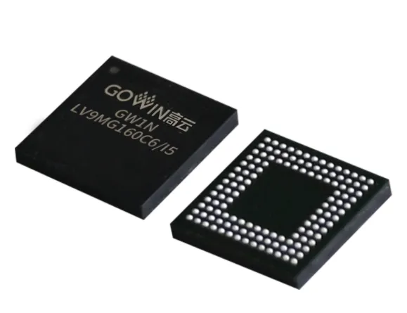
Gowin FPGA device package used as a component-level reference for programmable display and imaging data paths.

Validation & Testing

Validation & testing

Engineering-sample validation and production-test validation are handled as two separate layers with their own records.

  • Engineering-sample validation and production-test validation are handled as separate layers.
  • Workflows cover display output, interface communication, timing, sync, aging and batch consistency.
  • Test records, issue lists and revision suggestions carry the engineering result.
  • Performance figures require engineering test data or customer approval before they are published.
  • Power-on and basic communication

    Check power sequencing, board state, basic communication, abnormal recovery and the debug entry point.

  • Input/output interface stability

    Check the customer-defined input/output interfaces, connectors, cabling, transmission stability and boundary conditions.

  • Display output and timing

    Check display output, timing, refresh, sync and display-side control behaviour. Exact figures are confirmed against the project specification.

  • Aging and reliability

    Build test records around running stability, temperature, voltage, abnormal states and long-duration operation.

  • BOM and alternative parts

    Assess key component supply, alternatives, lifecycle, batch consistency and cost impact.

  • Production test and batch consistency

    Support test points, fixtures, workflow, pass criteria, issue closure and production handover.

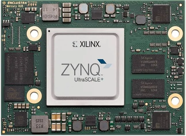
A Zynq UltraScale+ processing board used as an architecture reference for combined FPGA fabric and embedded processing.

Project inquiry

Turn display requirements into validated, manufacturable control hardware

Share display type, target specifications, interface requirements and project stage. We review the control hardware approach and ODM cooperation model; pricing and lead time follow project review.

Helpful to include

  • Screen size, pixel pitch, module layout and target resolution
  • Input source, control distance, sending/receiving count and cabling
  • Enclosure space, connector direction, power, temperature rise and service access
  • Test patterns, long-run checks, restart recovery and the factory-test standard
  • Existing boards, BOM, schematics or fault samples, if any
  • Estimated volume, project stage and target schedule